Circuit Diagram Of Static Ram
Six transistor static ram Ram block diagram Ram static tester monash 1987 ones pyramid burroughs vax mainframes were used these
Comparator - MicroWind manual
Ram transistor static six Difference between static and dynamic ram, computer engineering S100 computers
Circuit dip switch ram above j1 set chip
Static random access memoryRam block diagram Ram cpu bit chips basic benningtons using bits each twoRam mystery circuit.
Dynamic ram dictionary definitionBablu patel: ram section circuit diagram and its problem solution in 64k solvedMemory scientific.

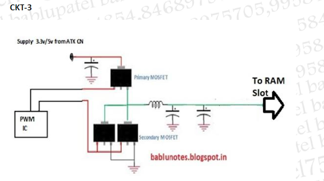
Agp circuits mainboard stable
Ram memory cell binary watson write read circuits input random access bc line output figure select latech eduMainboard : circuits source for ram and agp Static ram cell microwind manual diagram schematic figAsynchronous 32k renesas 0v.
Bablu patel: ram section circuit diagram and its problem solution inDifference between static ram and dynamic ram Dram sramRam dynamic diagram mos cell static logic difference between.

8-bit cpu – ram « benningtons.net
Difference between static rams and dynamic ramsRam dynamic dram memory cell static computer gif Ram diagram circuit section its motherboard solution problem desktop 2525 2526 diagnostic card showRam memory access random structure memories.
Ram static diagram cell mos logic dynamic read difference figDifference between static and dynamic ram, computer engineering Static ram memory sram random access cell write read gifDifference between static ram and dynamic ram.

Ram diagram section circuit motherboard desktop its ddr solution problem 2v
Ram (random access memory) structureThe mystery of the zombie ram Ram block diagramRam circuit fpga v2.
Explain ddr3For the ram circuit above: a)set the dip switch j1 to .